- 您现在的位置:买卖IC网 > Sheet目录1995 > FT10001L6X (Fairchild Semiconductor)IC RESET TIMER 6-MICROPAK
2011 Fairchild Semiconductor Corporation
www.fairchildsemi.com
FT10001 Rev 1.0.1
2
FT10001
—
Reset
Timer
with
Fixed
Delay
and
Reset
Pulse
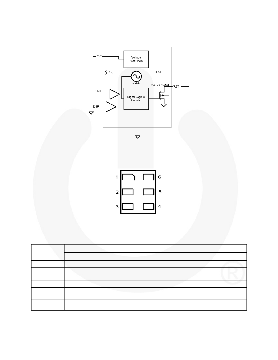
Block Diagram
Figure 1.
Block Diagram
Pin Configuration
Figure 2.
Pad Assignments (Top-Through View)
Pin Definitions
Pin #
Name
Description
Normal Operation
Zero-Second Factory-Test Mode
1
/RST1
Open-drain output, active LOW
2
GND
3
/SR0
Reset input with integrated pull-up, active LOW Reset input with integrated pull-up, active LOW
4
VCC
Power supply
5
DSR
Delay selection input; tie to GND during normal
operation
.(1)
Delay selection input. Pull HIGH to enable Zero-
second delay for factory test.
6
TEST
Used for device testing; tie to GND during
normal operation.
Used for device testing; tie to GND during normal
operation.
Note:
1.
This pin must always be tied to either GND or VCC. It must not float.
发布紧急采购,3分钟左右您将得到回复。
相关PDF资料
FT3001MPX
IC RESET TIMER 8-MLP
FT7521L6X
IC RESET TIMER 7.5SEC 6MICROPAK
FT7522L6X
IC RESET TIMER 6-MICROPAK
FT8010UMX
IC RESET TIMER CONF DELAY 10UMLP
FTS125-COO-010.0M
IC GPS BASED TIMING MOD (OCXO)
FTS125-CTV-010.0M
IC GPS BASED TIMING MOD (TCXO)
FTS250-010.0M
IC GPS BASED TIMING MOD (TCXO)
FTS375-010.0M
IC GPS BASED TIMING MOD (OCXO)
相关代理商/技术参数
FT100-02
制造商:HAKKO Corporation 功能描述:
FT100-03
制造商:HAKKO Corporation 功能描述:
FT100-04
制造商:HAKKO Corporation 功能描述:
FT100-04-230120
制造商:ITW Pancon 功能描述:
FT100-06
制造商:HAKKO Corporation 功能描述:
FT1000A
制造商:POWEREX 制造商全称:Powerex Power Semiconductors 功能描述:Phase Control SCR 1000 Amperes Avg 800-2500 Volts
FT1000A-16
制造商:POWEREX 制造商全称:Powerex Power Semiconductors 功能描述:Phase Control SCR 1000 Amperes Avg 800-2500 Volts
FT1000A-20
制造商:POWEREX 制造商全称:Powerex Power Semiconductors 功能描述:Phase Control SCR 1000 Amperes Avg 800-2500 Volts